For my project, I will design and simulate a VLSI circuit to compute
the 1-D Inverse Discrete Cosine Transformation. The IDCT is the basis of
many lossy compression algorithms, such as the JPEG standard for still images,
the MPEG video standard, and the MPEG audio standards. My IDCT circuit will
be targeted for use in an MPEG video decompression board.
Specifications
In MPEG video (as well as JPEG images), the video frame is divided
into 8x8 pixel blocks, and the Discrete Cosine Transform is
applied to each block individually. Because the DCT and IDCT are
separable, the 2-D transform is obtained by applying the 1-D DCT
or IDCT
to each row and then to each column of the 8x8 pixel block. My
circuit will be an implementation of an 8-pixel 1-D IDCT, which
can be used successively by the external circuitry to perform
a 2-D transform.
The I/O signals to the circuit will be:
- Vcc, ground
- clock signal
- 12 input lines
- 8 output lines
- BUSY output signal
- ENABLE input signal
As shown, the chip will have the standard power, ground, and clock
signals. An ENABLE input allows the external circuitry to
control the operation of the decoder. On the next eight clock
cycles after ENABLE goes high, the chip will read in the 8
DCT coefficients. It will then compute the transform,
lowering BUSY to indicate when the results are ready to be
placed on the output lines. In MPEG the largest DCT
coefficients are 12 bits, and the largest pixel values are 8
bits wide.
Design
My circuit will probably use the IDCT algorithm published by Loeffler,
Ligtenberg & Moschytz[1] (a C implementation of this
algorithm is available at [3]). I have chosen this algorithm
because it is simple and I have worked with it in the past
for performing the IDCT in software. However I will also
research other IDCT algorithms in case there is one that
would be faster or more natural when implemented in
VLSI. The algorithm works by successively computing on an array of 8
numbers, and then replacing the array with the output of each
computation. To obtain an item in the output array, two (or fewer)
elements are multiplied by a constant, then added or subtracted
together, and then a shift is performed on the result.
Figure 1 shows a block diagram of the circuit. The circuit contains
8x12 bit register files which store the inputs and outputs of each
succession of the algorithm, respectively. The input register file has
the special requirement that it is capable of outputing two different
registers simultaneously. There are two multipliers for multiplying
array items by constants, an addition/subtraction block, a 1-bit
right/left shifter, and multiplexers to route data signals
appropriately. The CONTROL block is a state machine which coordinates
all of the control signals to the other blocks.
The addition blocks will be simple 12-bit ripple carry adders, and the
multiplication block will use a successive shift-and-add algorithm. If
I have time, I can work on improving the performance of these blocks.
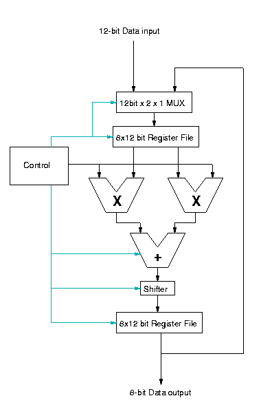
Figure 1: Block diagram for system
References
[1] Loeffler, Ligtenberg and Moschytz, "Practical Fast 1-D DCT
Algorithms with 11 Multiplications", Proceedings of the International
Conference on Acoustics, Speech, and Signal Processing 1989, pp. 988-991.
[2] Gonzalez, Rafael C. and Richard E. Woods. Digital Image
Processing. New York: Addison-Wesley Publishing Company, 1993.
[3] Web Page: http://www.cs.uow.edu.au/people/nabg/MPEG/IDCT.html
David J Crandall
Last modified: Sun Sep 12 14:40:50 EDT 1999