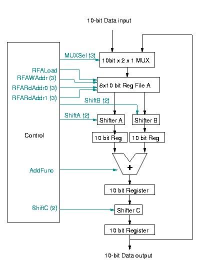
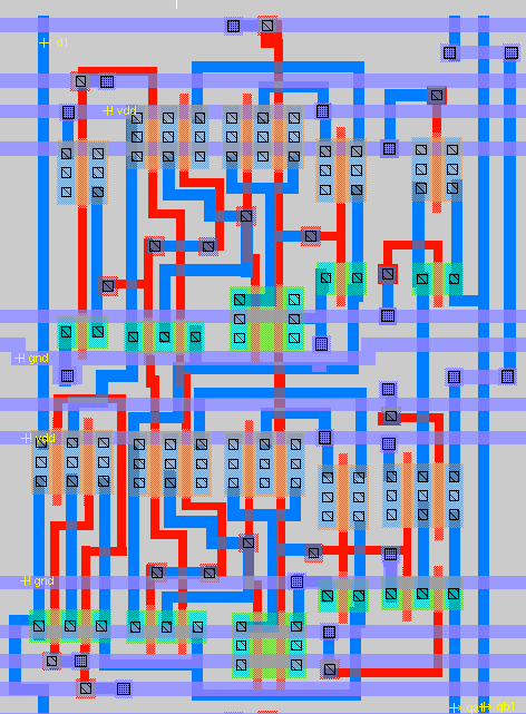
Figure 1: Updated block diagram of IDCT system
This project prototype report discusses the implementation of a Discrete Cosine Transform decoder in VLSI. First, the report will review the specifications for the chip, as well as the modifications to the design that have been made since the second interim report. Then, each sub-cell of the block will be covered, giving the implementation details and results of each. The current status of the project is that all sub-cells have been implemented in MAX, and have been verified in both IRSIM and HSPICE.
This chip will compute an approximation of the one dimensional Inverse Discrete Cosine Transformation on eight 10-bit signed integers. The operation of the chip is summarized as follows:
On the first 8 clock cycles, the eight DCT coefficients are read in one-by-one via the chip's 10-bit input.
The chip performs the IDCT on this data, and raises its READY output when the computation is complete.
The eight words of the result are placed one at a time on the 10-bit output during the next 8 clock cycles.
An updated block diagram for the circuit is shown in Figure 1.
The main modification made in the block diagram since the last report was the elimination of the second register file using a pipeline approach. The original block diagram required two register files, because each iteration of the algorithm needs to compute a new 8-integer array using the values stored in another 8-integer array. This design was not ideal because (1) register files consumes more area than any other sub-cell on the chip, so using two register files nearly doubled the size of the circuit, and (2) eight clock cycles were required between iterations of the algorithm to transfer the contents of the second register file back to the first, which was inefficient.
Fortunately, we noticed a clever reordering of the the array computations in the algorithm which eliminatess the need to retain all of the items of the old array. Specifically, our reordering allows a given item in the "old" array to be overwritten with its "new" value after four clock cycles. Therefore we can eliminate the second register file and instead insert three register stages in the datapath. Since the setup time of the registers is about the same as the propagation delay of the shifters, this approach will probably not allow us to use a faster clock rate, which is the usual benefit of pipelining. However, by eliminating the register file, we gain other advantages:
The register file is replaced with just four registers, significantly reducing area requirements
The 10 control signals once required by the second register file are no longer needed
The 8-cycle transfers from the second register file to the first are eliminated, reducing the number of states for the system from 80 to 49
Due to the above two factors, the size of the ROM required in the control unit reduces from 80x26 (2080 bytes) to 49x18 (882 bytes).
Figure
1: Updated block diagram of IDCT system
Description: Our shifter has four modes of operation: shift 1-bit left, shift 1-bit right, copy input to output, and output 0s. The shifter is in effect a 4:1 multiplexer, choosing between the left bit, right bit, current bit, and ground, depending on the control signals. For implementation, a bit-sliced approach was used, consisting of pass transistors to either connect the output to the left bit, the right bit, the current bit, or to ground.
Input Signals:
Input: 10-bit integer.
FUNC: 2-bit control signal indicating the function to perform.
Output Signals:
O: 10-bit result of operation. If FUNC=00, Output=Input; if FUNC=01, Output=0; if FUNC=11, Output=Input arithmetic right-shifted 1 bit; if FUNC=10, Output=Input arithmetic left-shifted 1 bit.
Area: 82.44 x 14.5 micron
Cell Design: Dual PMOS/NMOS pass transistors are used to multiplex between the left bit input, the right bit input, and the current bit input. A single NMOS transistor is activated for the 0 function, which just pulls the output to ground. This arrangement requires 7 control signals: lsh, lshnot, rsh, rshnot, eq, eqnot, and zero. Standard dual CMOS logic is used to convert the FUNC input to the appropriate 7 control signals, using the equations:
lsh = FUNC1 and not FUNC0; lshnot=not lsh
rsh = FUNC1 and FUNC0; rshnot=not rsh
eq = not FUNC1 and not FUNC0; eqnot=not eq
zero = not FUNC1 and FUNC0
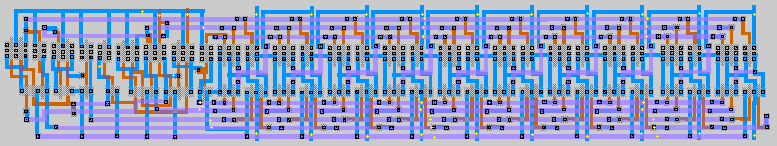
Figure 2 shows the transistor-level schematic for one bit-sliced cell, while figure 3 shows the MAX layout for a one-bit cell. Finally, figure 4 shows the full 10-bit shifter layout, including the CMOS circuitry that generates the control signals from the FUNC input.
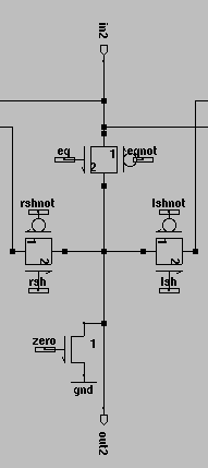 Figure 2: Transistor-level schematic of 1-bit shifter |
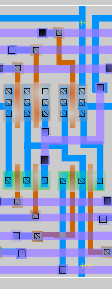 Figure 3: Layout of 1-bit shifter |
Figure
4: Layout of full 10-bit shifter, with control circuitry
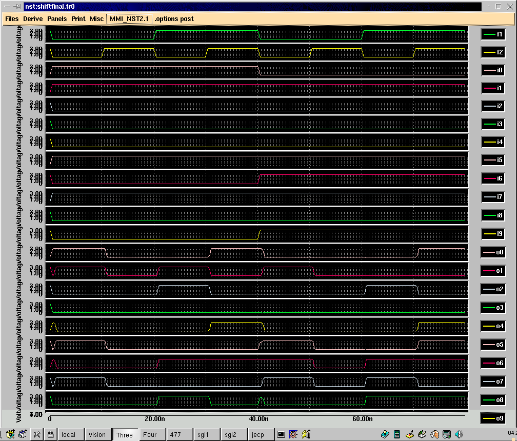
IRSIM simulation: Figures 5 and 6 show the IRSIM command file and simulation results, respectively, for the shifter. The command file tests all four function on two sample 10-bit inputs. As shown in the simulation results, the shifter performs correctly.
vector in i9 i8 i7 i6 i5 i4 i3 i2 i1 i0 vector out o9 o8 o7 o6 o5 o4 o3 o2 o1 o0 vector func f1 f2 w in out func set in 0010100011 set func 00 print equal func, out should = in s 1000 set func 01 print zero func, out should = 0 s 1000 set func 10 print lsh func, out should = in left shift 1 s 1000 set func 11 print rsh func, out should = in arithmetic right shift 1 s 1000 set in 1011100010 set func 00 print equal func, out should = in s 1000 set func 01 print zero func, out should = 0 s 1000 set func 10 print lsh func, out should = in left shift 1 s 1000 set func 11 print rsh func, out should = in arithmetic right shift 1 s 1000 exit |
equal func, out should = in func=00 out=0010100011 in=0010100011 time = 1000.00ns zero func, out should = 0 func=01 out=0000000000 in=0010100011 time = 2000.00ns lsh func, out should = in left shift 1 func=10 out=0101000110 in=0010100011 time = 3000.00ns rsh func, out should = in arithmetic right shift 1 func=11 out=0001010001 in=0010100011 time = 4000.00ns equal func, out should = in func=00 out=1011100010 in=1011100010 time = 5000.00ns zero func, out should = 0 func=01 out=0000000000 in=1011100010 time = 6000.00ns lsh func, out should = in left shift 1 func=10 out=0111000100 in=1011100010 time = 7000.00ns rsh func, out should = in arithmetic right shift 1 func=11 out=1101110001 in=1011100010 time = 8000.00ns |
HSPICE simulation: Figures 7 and 8 (figure 8 is located in appendix A) show the HSPICE command file and simulation results, respectively, for the shifter. The command file performs the same operations as the IRSIM command file described above. The HSPICE results confirm that the shifter does work as expected. We found that the worst-case delay is 948 pS. This occurs when the control signals change to left, right, or equal, and the input bit changes to 1, so that the output bit must be charged to 1.
VDD 3.3 CLK 10.0 RISE 0.5 FALL 0.5 i0 11110000 i1 11111111 i2 00000000 i3 00000000 i4 00000000 i5 11111111 i6 00001111 i7 11111111 i8 00000000 i9 00001111 f1 00110011 f2 01010101 |
Description: Our adder/subtractor performs 2's complement addition and subtraction on 10-bit signed integers. We used a simple ripple-carry adder, since more advanced types of adders would not provide much of a performance boost with only 10-bit arithmetic.
Input Signals:
A, B: 10-bit 2's complement signed integers to use as input.
FUNC: 0 if operands are to be added (A+B), 1 if they are to be subtracted (A-B)
Output Signals:
O: 10-bit result of operation.
Area: 87.47 x 21.3 micron
Cell Design: We used the static CMOS mirror adder presented in Rabaey p. 391. We refer the reader to this reference for a transistor-level diagram of the circuit. To allow subtraction, the B input is xor'ed with FUNC, and the carry-in of the adder is FUNC. This effectively takes the 2's complement of B when FUNC is 1, and performs normal addition otherwise. Figure 9 shows the layout of a 1-bit full adder/subtractor, and figure 10 shows the layout of the whole 10-bit unit.
IRSIM simulation: Figures 11 and 12 show the IRSIM command file and simulation results, respectively, for the adder/subtractor. The command file tests the addition and subtraction operations on several sample integers. The results show that the module performs correctly.
vector as a9 a8 a7 a6 a5 a4 a3 a2 a1 a0 vector bs b9 b8 b7 b6 b5 b4 b3 b2 b1 b0 vector os o9 o8 o7 o6 o5 o4 o3 o2 o1 o0 w as bs func funcnot os print 300 + 200 should equal 500 print (0100101100 + 0011001000 should equal 0111110100) l func h funcnot set as 0100101100 set bs 0011001000 s 1000 print 300 - 200 should equal 100 print (0100101100 - 0011001000 should equal 0001100100) h func l funcnot set as 0100101100 set bs 0011001000 s 1000 print 300 - -200 should equal 500 print (0100101100 - 1100111000 should equal 0111110100) h func l funcnot set as 0100101100 set bs 1100111000 s 1000 print 200 - 300 should equal -100 print (0011001000 - 0100101100 should equal 1110011100) h func l funcnot set as 0011001000 set bs 0100101100 s 1000 print 23 + 456 should equal 479 print (0000010111 + 0111001000 should equal 0111011111 l func h funcnot set as 0000010111 set bs 0111001000 s 1000 |
300 + 200 should equal 500 (0100101100 + 0011001000 should equal 0111110100) os=0111110100 bs=0011001000 as=0100101100 funcnot=1 func=0 time = 1000.00ns 300 - 200 should equal 100 (0100101100 - 0011001000 should equal 0001100100) os=0001100100 bs=0011001000 as=0100101100 funcnot=0 func=1 time = 2000.00ns 300 - -200 should equal 500 (0100101100 - 1100111000 should equal 0111110100) os=0111110100 bs=1100111000 as=0100101100 funcnot=0 func=1 time = 3000.00ns 200 - 300 should equal -100 (0011001000 - 0100101100 should equal 1110011100) os=1110011100 bs=0100101100 as=0011001000 funcnot=0 func=1 time = 4000.00ns 23 + 456 should equal 479 (0000010111 + 0111001000 should equal 0111011111 os=0111011111 bs=0111001000 as=0000010111 funcnot=1 func=0 time = 5000.00ns |
HSPICE simulation: Figures 13 and 14 (figure 14 is located in appendix A) show the HSPICE command file and simulation results, respectively, for the adder/subtractor. The command file performs the same operations as the IRSIM command file described above. The HSPICE results confirm that the adder/subtractor does work as expected.
The worst-case delay for a ripple carry adder is when the most significant bit requires a carry in rippling from the least significant bit. In our case 1 - 1 is the worst case. Using an HSPICE simulation, we found the worst case delay to be 3.88 ns.
VDD 3.3 CLK 10.0 RISE 0.5 FALL 0.5 a9 0000000 a8 1110000 a7 0001000 a6 0001000 a5 1110000 a4 0000100 a3 1111000 a2 1110100 a1 0000100 a0 0000111 b9 0010011 b8 0011111 b7 1100111 b6 1100111 b5 0011011 b4 0010011 b3 1111111 b2 0001011 b1 0000011 b0 0000011 func 0111001 funcnot 1000110 |
Description: Our register file consists of 8 10-bit registers. On a given clock cycle, any register may be written to, and any two registers may be read from. All registers may be cleared to 0 using an asynchronous active-low reset. We use the positive-edge-triggered D-flip-flop developed in Lab #3 for our register file, with some modifications, including an output enable and two output ports.
Input Signals:
RA2, RA1, RA0: address of register whose contents will be placed on output port A
RB2, RB1, RB0: address of register whose contents will be placed on output port B
CLK: clock signal
RESET: asynchronous active-low reset which clears all registers to 0
W2, W1, W0: address of register which will be written to on next clock pulse
WENB: write enable: write to register file if W2W1W0 is nonzero and WENB is nonzero
D9...D0: data which will be written to register W2W1W0 on next clock pulse
Output Signals:
QA9...QA0: output port A: contents of register specified by RA inputs
QB9...QB0: output port B: contents of register specified by RB inputs
Area: 199.6 x 174.9 micron
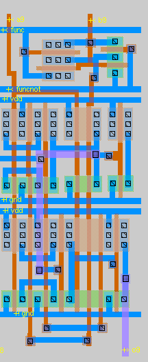
Cell Design: The basic building block of the register file is the D-flip-flop developed in Lab #3. It is a positive-edge-triggered, active-low-reset D flip-flop. A master-slave approach with two D latches are used to create the flip-flop. Since we are using D latches and not JK latches, the flip-flop does not suffer from the input glitch problem that occurs with JK latches in master-slave arrangements. The reader is referred to our Lab #3 report for more details about the basic D flip-flop. The D-flip-flop was modified to have two output ports which can be enabled or tri-stated based on control inputs. Also a write enable input was added. In both cases, NMOS/PMOS pass transistors were used to implement this new functionality, requiring 6 additional transistors total. Figure 15 shows the updated transistor diagram for our D flip-flops, while figure 16 shows the MAX layout.
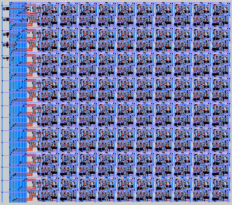
The register file is essentially an 8x10 array of D flip-flops. The enable control signals for each row are tied together. The output signals for each column are tied together, as are the data inputs. All clocks and resets of all D-flip-flops are connected. Finally, three 3:8 decoder are used to generate the two read enable signals and write enable signal for each row of the register file. A simple static dual CMOS implementation of the decoder is used, using inverters and NAND gates. Figure 17 shows the MAX layout of the register file. The 8x10 array of D-flip-flops is clearly visible, and the portion on the left are the decoders.
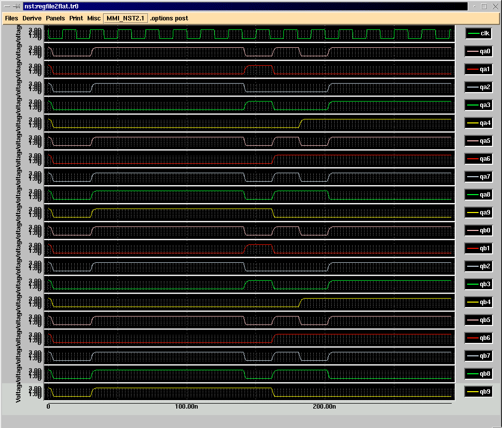
IRSIM simulation: Figures 18 and 19 show the IRSIM command file and simulation results, respectively, for the register file. The command file performs a sequence of writes to different registers in the register file, and then reads out the contents of the registers. As can be seen from the output, the register file works correctly in doing these operations.
vector din d9 d8 d7 d6 d5 d4 d3 d2 d1 d0 vector qa qa9 qa8 qa7 qa6 qa5 qa4 qa3 qa2 qa1 qa0 vector qb qb9 qb8 qb7 qb6 qb5 qb4 qb3 qb2 qb1 qb0 vector radda ra2 ra1 ra0 vector raddb rb2 rb1 rb0 vector w w2 w1 w0 w din qa qb radda raddb w reset clk wenb l reset l clk l wenb set din 0000000000 set w 000 set radda 000 set raddb 000 stepsize 1000 clock clk 0 1 c c c h reset print all registers should be cleared c set wenb 1 print write 1110100101 to register 0 set din 1110100101 set w 000 c print write 1000001010 to register 1 set din 1000001010 set w 001 c print write 0111100001 to register 2 set din 0111100001 set w 010 c print write 0101010000 to register 3 set din 0101010000 set w 011 c print write 0011111101 to register 4 set din 0011111101 set w 100 c print write 0010010010 to register 5 set din 0010010010 set w 101 c print write 0100100100 to register 6 set din 0100100100 set w 110 c print write 1000001000 to register 7 set din 1000001000 set w 111 c print don't do anything (test wenb) l wenb set w 000 c print output reg0 on port a, reg1 on port b print should be a= 1110100101, b= 1000001010 set radda 000 set raddb 001 c print output reg2 on port a, reg3 on port b print should be a= 0111100001, b= 0101010000 set radda 010 set raddb 011 c print output reg4 on port a, reg5 on port b print should be a= 0011111101, b= 0010010010 set radda 100 set raddb 101 c print output reg6 on port a, reg7 on port b print should be a= 0100100100, b= 1000001000 set radda 110 set raddb 111 c |
w=000 raddb=000 radda=000 qb=0000000000 qa=0000000000 din=0000000000 wenb=0 clk=1 reset=0 time = 2000.00ns w=000 raddb=000 radda=000 qb=0000000000 qa=0000000000 din=0000000000 wenb=0 clk=1 reset=0 time = 4000.00ns w=000 raddb=000 radda=000 qb=0000000000 qa=0000000000 din=0000000000 wenb=0 clk=1 reset=0 time = 6000.00ns all registers should be cleared w=000 raddb=000 radda=000 qb=0000000000 qa=0000000000 din=0000000000 wenb=0 clk=1 reset=1 time = 8000.00ns (regfile2.com,25): wenb: No such vector write 1110100101 to register 0 w=000 raddb=000 radda=000 qb=0000000000 qa=0000000000 din=1110100101 wenb=0 clk=1 reset=1 time = 10000.00ns write 1000001010 to register 1 w=001 raddb=000 radda=000 qb=0000000000 qa=0000000000 din=1000001010 wenb=0 clk=1 reset=1 time = 12000.00ns write 0111100001 to register 2 w=010 raddb=000 radda=000 qb=0000000000 qa=0000000000 din=0111100001 wenb=0 clk=1 reset=1 time = 14000.00ns write 0101010000 to register 3 w=011 raddb=000 radda=000 qb=0000000000 qa=0000000000 din=0101010000 wenb=0 clk=1 reset=1 time = 16000.00ns write 0011111101 to register 4 w=100 raddb=000 radda=000 qb=0000000000 qa=0000000000 din=0011111101 wenb=0 clk=1 reset=1 time = 18000.00ns write 0010010010 to register 5 w=101 raddb=000 radda=000 qb=0000000000 qa=0000000000 din=0010010010 wenb=0 clk=1 reset=1 time = 20000.00ns write 0100100100 to register 6 w=110 raddb=000 radda=000 qb=0000000000 qa=0000000000 din=0100100100 wenb=0 clk=1 reset=1 time = 22000.00ns write 1000001000 to register 7 w=111 raddb=000 radda=000 qb=0000000000 qa=0000000000 din=1000001000 wenb=0 clk=1 reset=1 time = 24000.00ns don't do anything (test wenb) w=000 raddb=000 radda=000 qb=0000000000 qa=0000000000 din=1000001000 wenb=0 clk=1 reset=1 time = 26000.00ns output reg0 on port a, reg1 on port b should be a= 1110100101, b= 1000001010 w=000 raddb=001 radda=000 qb=1000001010 qa=0000000000 din=1000001000 wenb=0 clk=1 reset=1 time = 28000.00ns output reg2 on port a, reg3 on port b should be a= 0111100001, b= 0101010000 w=000 raddb=011 radda=010 qb=0101010000 qa=0111100001 din=1000001000 wenb=0 clk=1 reset=1 time = 30000.00ns output reg4 on port a, reg5 on port b should be a= 0011111101, b= 0010010010 w=000 raddb=101 radda=100 qb=0010010010 qa=0011111101 din=1000001000 wenb=0 clk=1 reset=1 time = 32000.00ns output reg6 on port a, reg7 on port b should be a= 0100100100, b= 1000001000 w=000 raddb=111 radda=110 qb=1000001000 qa=0100100100 din=1000001000 wenb=0 clk=1 reset=1 time = 34000.00ns |
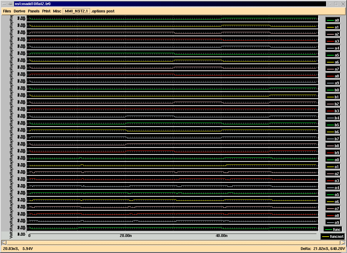
HSPICE simulation: Figures 20 and 21 (figure 21 is located in appendix A) show the HSPICE command file and simulation results, respectively, for the register file. The command file performs approximately the the same operations as the IRSIM command file described above, except that the operations have been simplified to allow for faster simulation time. In the HSPICE command file, register 0 through 4 are loaded with the same values as in the IRSIM command file, and then these four registers are output on both the a and b ports in sequence. The results are correct and can be verified by comparing the outputs to the values input to the registers (shown in figures 18 and 19). Note: To promote readability, only the output signals are shown in the NST graph.
The worst-case delay for the register file is 2.76 ns, which corresponds to the time it takes a 1 to propagate to the output, after the read address lines have changed.
VDD 3.3 CLK 10.0 RISE 0.5 FALL 0.5 d9 001100000110000 d8 001011001000000 d7 001010110000000 d6 000011100000000 d5 001010101000000 d4 000001110000000 d3 000100100110000 d2 001000101000000 d1 000100010000000 d0 001010100000000 ra2 000000000000011 ra1 000000000000101 ra0 000000000000000 rb2 000000000000011 rb1 000000000000101 rb0 000000000001111 w2 000000111100000 w1 000011001100000 w0 000101010100000 reset 001111111111111 wenb 001111111100000 |
Control Unit
Description: The control unit is a finite state machine which generates the control signals, instructing the various sub-cells to interact correctly. The control unit is composed of a counter and a ROM. The control unit can be reset to its initial state by pulling its RESET input low. As long as RESET is high and clock pulses are provided, the control unit moves through the words of the ROM, outputting one per cycle. Since the IDCT requires the same steps in the same order regardless of input, there is no input to the finite state machine. The machine always moves through its states in the same order.
Input Signals:
CLK: clock signal
RESET: asynchronous active-low reset which clears all registers to 0
Output Signals:
READY: Set high to indicate to external circuitry when IDCT is complete.
MUXSEL: Select input to 10bitx2x1 MUX.
RFALoad: Connected to LOAD signal of Register File A.
RFAWAddr: Connected to WADDR input of Register File A.
RFARdAddr0: Connected to RAddr0 input of Register File A.
RFARdAddr1: Connected to RAddr1 input of Register File A.
ShiftA, ShiftB, ShiftC: Control signals for shifters.
Area: total: 65.7 x 111.2 micron (individual sub-cells: address incrementer: 41.39 x 11.69; address register: 65.7 x 21.14; ROM: 48.94 x 76.33)
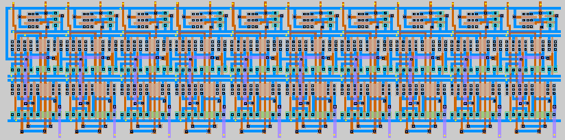
Cell Design: The first step in designing the control unit was to write the microcode needed by the circuit. Figure 22 (located in Appendix A) shows the microcode, in binary format with human-readable comments on the right. A 49 word ROM with 18 bit words is required to store the microcode. A Psuedo-NMOS NOR ROM was implemented, similar to the one presented in Rabaey pp. 562-563. For the address decoder of the ROM, we used a NOR decoder similar to that present in Rabaey pp. 592. We refer the reader to these pages to see transistor schematics and layouts of the individual cells. We implemented Pseudo-NMOS versions of both the ROM and the decoder instead of dynamic logic, meaning that the gate of the pull-up transistor is always grounded. Although this is non-ideal from a power perspective (since a path from VDD to ground exists), we decided to do this for the sake of simplicity.
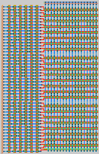
The ROM was programmed by hand using MAX, by deleting contacts and transistors whenever a 1 was desired. The ROM layout in MAX is shown in figure 23. The left portion of the ROM is the address decoder, and the right portion is the ROM itself.
Since we require 49 words in the ROM, we need 6-bit addresses. The 6-bit counter used in the control unit is based on the 4-bit counter implemented for our Lab #3 assignment. It consists of an increment unit, which contains 6 bit-sliced half-adders, and a 6-bit register similar to the ones used in the register file. We refer the reader to our Lab #3 report for more information about the design of the counter.
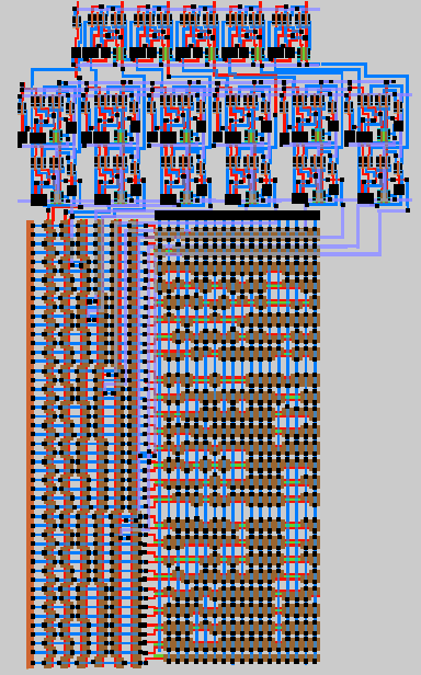
Figure 24 shows the full layout of the control unit.
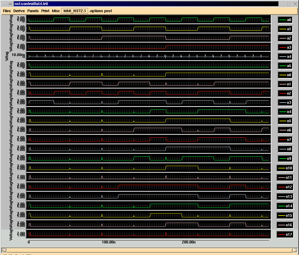
IRSIM simulation: Figures 25 and 26 show the IRSIM command file and simulation results, respectively, for the control unit. The command file is simple a sequence of clock pulses, so that the control module goes through all of its 49 states. The outputs have been verified as correct by comparing them to the microcode shown in figure 22.
vector add a5 a4 a3 a2 a1 a0 vector out o0 o1 o2 o3 o4 o5 o6 o7 o8 o9 o10 o11 o12 o13 o14 o15 o16 o17 w add out stepsize 1000 clock clk 0 1 l reset c c h reset c c c c c c c c c c c c c c c c c c c c c c c c c c c c c c c c c c c c c c c c c c c c c c c c |
out=000100000000000000 add=000000 time = 2000.00ns out=000100000000000000 add=000000 time = 4000.00ns out=001000000000000000 add=000001 time = 6000.00ns out=010000000000000000 add=000010 time = 8000.00ns out=011000000000000000 add=000011 time = 10000.00ns out=000000000000000000 add=000100 time = 12000.00ns out=011100000000110000 add=000101 time = 14000.00ns out=010100100100110000 add=000110 time = 16000.00ns out=001110110000111100 add=000111 time = 18000.00ns out=100001101010111110 add=001000 time = 20000.00ns out=100101001110111010 add=001001 time = 22000.00ns out=101111011100000000 add=001010 time = 24000.00ns out=111011111000000000 add=001011 time = 26000.00ns out=110010010100111010 add=001100 time = 28000.00ns out=110100000100001000 add=001101 time = 30000.00ns out=111100100000001000 add=001110 time = 32000.00ns out=100101100000011010 add=001111 time = 34000.00ns out=100011011100001000 add=010000 time = 36000.00ns out=101011011100000010 add=010001 time = 38000.00ns out=111000100000011100 add=010010 time = 40000.00ns out=100110010100001100 add=010011 time = 42000.00ns out=111110010100010000 add=010100 time = 44000.00ns out=101000000000011110 add=010101 time = 46000.00ns out=100001000000011100 add=010110 time = 48000.00ns out=101100000000010000 add=010111 time = 50000.00ns out=101000100000010000 add=011000 time = 52000.00ns out=110111011100000000 add=011001 time = 54000.00ns out=100110101100000000 add=011010 time = 56000.00ns out=101010101100001110 add=011011 time = 58000.00ns out=111111011100001100 add=011100 time = 60000.00ns out=100001010000001110 add=011101 time = 62000.00ns out=110001010000001100 add=011110 time = 64000.00ns out=111101001100001110 add=011111 time = 66000.00ns out=100001001100001100 add=100000 time = 68000.00ns out=110000000100001110 add=100001 time = 70000.00ns out=100000000100001110 add=100010 time = 72000.00ns out=100111011100001100 add=100011 time = 74000.00ns out=111111011100001100 add=100100 time = 76000.00ns out=101110010100001110 add=100101 time = 78000.00ns out=110110010100001110 add=100110 time = 80000.00ns out=111000000000011100 add=100111 time = 82000.00ns out=101100100000011100 add=101000 time = 84000.00ns out=110001000000010001 add=101001 time = 86000.00ns out=100001100000010000 add=101010 time = 88000.00ns out=100010000000010000 add=101011 time = 90000.00ns out=100010100000010000 add=101100 time = 92000.00ns out=100011000000010000 add=101101 time = 94000.00ns out=100011100000010000 add=101110 time = 96000.00ns out=100000000000000000 add=101111 time = 98000.00ns out=100000000000000000 add=110000 time = 100000.00ns |
HSPICE simulation: The HSPICE command file and simulation results for the control module are shown in figures 27 and 28 (figure 28 is located in Appendix A), respectively. The command file simply takes the control unit through its first 10 states, showing the first 10 control outputs. The results have been verified by comparing them to the microcode shown in figure 22.
The maximum propagation delay for the ROM was found to be 684.21 pS, corresponding to a high-to-low transition in the output of a bit in the ROM. We also noted that the voltage swing on the outputs was reduced to 1.0 volts for low and 3.3 volts for high. This is because we are using a form of ratioed logic. For our purposes, 1.0 volts is a low enough value to prevent noise problems. We will introduce a buffer stage when we connect the ROM's outputs to the external circuitry in order to prevent noise problems.
VDD 3.3 CLK 10.0 RISE 0.5 FALL 0.5 clk 010101010101010101010101010101 reset 0011111111111111111111 |
Description: Our block diagram calls for a multiplexer, to allow the register file to be written to by either the chip inputs or by the final register of the pipeline. However, an explicit multiplexer is not really needed. The registers have enable inputs, so we can simply insert a pass transistor tri-state buffer on the chip input signals. The multiplexer is then replaced by simply turning on either the enable for the register or the enable for the tri-state buffer.
M R R R R S S S A R U F F F F A B C D E X A A A A D A S L W R R M D E D A A A D Y L 0 1 #### load data from input (8 cycles) 0 1 001 xxx xxx xx xx xx x 0 0 1 010 xxx xxx xx xx xx x 0 0 1 100 xxx xxx xx xx xx x 0 0 1 110 xxx xxx xx xx xx x 0 0 1 000 xxx xxx xx xx xx x 0 0 1 111 000 000 00 11 xx x 0 # R0a <- Rf0, R0b <- Rf0/2 0 1 101 001 001 00 11 xx 0 0 # R0a <- Rf1, R0b <- Rf1/2, R1 <- R0a+R0b 0 1 011 101 100 00 11 11 0 0 # s2[3] # R2 <- R1/2, R1 <- R0a+R0b, R0a <- Rf5, R0b <- Rf4/2 1 1 000 011 010 10 11 11 1 0 # s2[6] # Rf0 <- R2, R2 <- R1/2, R1 <- R0a-R0b, R0a <- Rf3*2, R0b <- Rf2/2 1 1 001 010 011 10 11 10 1 0 # s2[4] # Rf1 <- R2, R2 <- R1*2, R1 <- R0a-R0b, R0a <- Rf2*2, R0b <- Rf3/2 1 1 011 110 111 00 00 00 0 0 # s2[5] # Rf3 <- R2, R2 <- R1, R1 <- R0a+R0b, R0a <- Rf6, R0b <- Rf7 1 1 110 111 110 00 00 00 0 0 # s2[7] # Rf6 <- R2, R2 <- R1, R1 <- R0a+R0b, R0a <- Rf7, R0b <- Rf6 1 1 100 100 101 00 11 10 1 0 # s2[1] # Rf4 <- R2, R2 <- R1*2, R1 <- R0a-R0b, R0a <- Rf4, R0a <- Rf5/2 1 1 101 000 001 00 00 10 0 0 # s2[0] # Rf5 <- R2, R2 <- R1*2, R1 <- R0a+R0b, R0a <- Rf0, R0b <- Rf1 1 1 111 001 000 00 00 10 0 0 # s2[2] # Rf7 <- R2, R2 <- R1*2, R1 <- R0a+R0b, R0a <- Rf1, R0b <- Rf0 1 1 001 011 xxx 00 01 10 1 0 # s3[6] # Rf1 <- R2, R2 <- R1*2, R1 <- R0a-R0b, R0a <- Rf3, R0b <- 0 1 1 000 110 111 00 00 10 x 0 # s3[1] # Rf0 <- R2, R2 <- R1*2, R1 <- R0a+R0b, R0a <- Rf6, R0b <- Rf7 1 1 010 110 111 00 00 00 1 0 # s3[7] # Rf2 <- R2, R2 <- R1, R1 <- R0a-R0b, R0a <- Rf6, R0b <- Rf7 1 1 110 001 xxx 00 01 11 0 0 # s3[4] # Rf6 <- R2, R2 <- R1/2, R1 <- R0a+R0b, R0a <- Rf1, R0b <- 0 1 1 001 100 101 00 00 11 x 0 # s3[0] # Rf1 <- R2, R2 <- R1/2, R1 <- R0a+R0b, R0a <- Rf4, R0b <- Rf5 1 1 111 100 101 00 01 00 0 0 # s3[3] # Rf7 <- R2, R2 <- R1, R1 <- R0a+R0b, R0a <- Rf4, R0b <- Rf5 1 1 010 000 xxx 00 01 11 1 0 # s3[2] # Rf2 <- R2, R2 <- R1/2, R1 <- R0a-R0b, R0a <- Rf0, R0b <- 0 1 1 000 010 xxx 00 01 11 x 0 # s3[5] # Rf0 <- R2, R2 <- R1/2, R1 <- R0a+R0b, R0a <- Rf2, R0b <- 0 1 1 011 000 xxx 00 01 00 x 0 # s5[1] # Rf3 <- R2, R2 <- R1, R1 <- R0a+R0b, R0a <- Rf0, R0b <- 0 1 1 010 001 xxx 00 01 00 x 0 # s5[5] # Rf2 <- R2, R2 <- R1, R1 <- R0a+R0b, R0a <- Rf1, R0b <- 0 1 1 101 110 111 00 00 00 x 0 # s5[3] # Rf5 <- R2, R2 <- R1, R1 <- R0a+R0b, R0a <- Rf6, R0b <- Rf7 1 1 001 101 011 00 00 00 0 0 # s5[6] # Rf1 <- R2, R2 <- R1, R1 <- R0a+R0b, R0a <- Rf5, R0b <- Rf3 1 1 010 101 011 00 00 11 1 0 # s5[2] # Rf5 <- R2, R2 <- R1/2, R1 <- R0a-R0b, R0a <- Rf5, R0b <- Rf3 1 1 111 110 111 00 00 11 0 0 # s5[7] # Rf3 <- R2, R2 <- R1/2, R1 <- R0a+R0b, R0a <- Rf6, R0b <- Rf7 1 1 000 010 100 00 00 11 1 0 # s5[0] # Rf6 <- R2, R2 <- R1/2, R1 <- R0a-R0b, R0a <- Rf2, R0b <- Rf4 1 1 100 010 100 00 00 11 0 0 # s5[4] # Rf2 <- R2, R2 <- R1/2, R1 <- R0a+R0b, R0a <- Rf2, R0b <- Rf4 1 1 111 010 011 00 00 11 1 0 # s6[2] # Rf7 <- R2, R2 <- R1/2, R1 <- R0a-R0b, R0a <- Rf2, R0b <- Rf3 1 1 000 010 011 00 00 11 0 0 # s6[1] # Rf0 <- R2, R2 <- R1/2, R1 <- R0a+R0b, R0a <- Rf2, R0b <- Rf3 1 1 100 000 001 00 00 11 1 0 # s6[7] # Rf4 <- R2, R2 <- R1/2, R1 <- R0a-R0b, R0a <- Rf0, R0b <- Rf1 1 1 000 000 001 00 00 11 1 0 # s6[0] # Rf2 <- R2, R2 <- R1/2, R1 <- R0a-R0b, R0a <- Rf0, R0b <- Rf1 1 1 001 110 111 00 00 11 0 0 # s6[5] # Rf1 <- R2, R2 <- R1/2, R1 <- R0a+R0b, R0a <- Rf6, R0b <- Rf7 1 1 111 110 111 00 00 11 0 0 # s6[6] # Rf7 <- R2, R2 <- R1/2, R1 <- R0a+R0b, R0a <- Rf6, R0b <- Rf7 1 1 011 100 101 00 00 11 1 0 # s6[3] # Rf0 <- R2, R2 <- R1/2, R1 <- R0a-R0b, R0a <- Rf4, R0b <- Rf5 1 1 101 100 101 00 00 11 1 0 # s6[4] # Rf5 <- R2, R2 <- R1/2, R1 <- R0a-R0b, R0a <- Rf4, R0b <- Rf5 1 1 110 000 xxx 00 01 11 0 0 # # Rf6 <- R2, R2 <- R1/2, R1 <- R0a+R0b, R0a <- Rf0, R0b <- 0 1 1 011 001 xxx 00 01 11 x 0 # # Rf3 <- R2, R2 <- R1/2, R1 <- R0a+R0b, R0a <- Rf1, R0b <- 0 1 1 100 010 xxx 00 01 00 x 1 # # Rf4 <- R2, R2 <- R1, R1 <- R0a+R0b, R0a <- Rf2, R0b <- 0 1 0 000 011 xxx 00 01 00 x 0 # # R2 <- R1, R1 <- R0a+R0b, R0a <- Rf3, R0b <- 0 1 0 000 100 xxx 00 01 00 x 0 # # R2 <- R1, R1 <- R0a+R0b, R0a <- Rf4, R0b <- 0 1 0 000 101 xxx 00 01 00 x 0 # # R2 <- R1, R1 <- R0a+R0b, R0a <- Rf5, R0b <- 0 1 0 000 110 xxx 00 01 00 x 0 # # R2 <- R1, R1 <- R0a+R0b, R0a <- Rf6, R0b <- 0 1 0 000 111 xxx 00 01 00 x 0 # # R2 <- R1, R1 <- R0a+R0b, R0a <- Rf7, R0b <- 0 1 0 000 xxx xxx xx xx 00 x 0 # # R2 <- R1, R1 <- R0a+R0b 1 0 000 xxx xxx xx xx 00 x 0 # # R2 <- R1 |